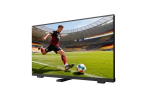
Explore our precision-engineered LED display panels, optimized for high pixel density, extreme contrast ratios, and continuous operational durability.
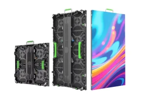
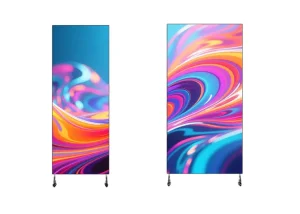
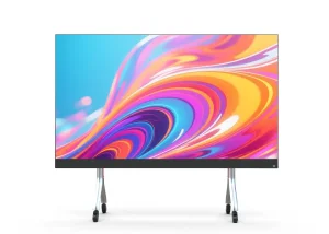
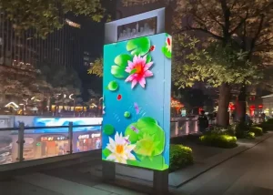
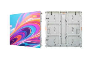

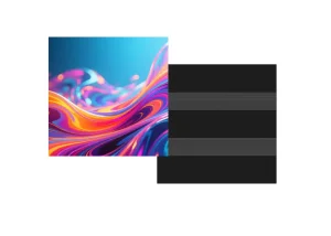

In modern Optoelectronics, LED display pixel density defines the spatial resolution limit, modulated directly by the center-to-center distance between adjacent diode clusters (Pixel Pitch, denoted as P in millimeters). As global procurement demands transition from standard definition display boards to hyper-immersive 4K, 8K, and MicroLED video walls, evaluating pixel density requires an intimate understanding of spatial frequency, fill factor, and human visual acuity metrics.
Pixel density per square meter ($D_{sqm}$) is inversely proportional to the square of the pixel pitch ($P$):
For instance, reducing pitch from P2.5 to P1.25 increases pixel density fourfold from 160,000 to 640,000 pixels/m².
The minimum comfortable viewing distance ($D_{min}$) where discrete pixels blend into a seamless image relies on human Snellen visual acuity (1 arcminute angle):
For optimal visual performance ($D_{opt}$), enterprise engineers apply a factor of $P \times 2.5$.
Fill factor measures the ratio of the light-emitting diode area to the total pixel area. Higher fill factor minimizes the 'screen-door effect' and glare.
Advanced Chip-on-Board (COB) packaging achieves a fill factor exceeding 90%, outperforming traditional SMD packaging (~40-50%).
The wholesale LED display manufacturing ecosystem is experiencing a massive paradigm shift. As conventional Surface Mount Device (SMD) encapsulation hits mechanical thermal limits at P1.2mm, advanced packaging technologies such as Flip-Chip COB (Chip on Board), GOB (Glue on Board), and MIP (MicroLED in Package) are redefining industry standards.
Legacy SMD encapsulation solders packaged LED lamps onto a PCB board. In ultra-fine pitch environments, SMD suffers from vulnerable solder joints and restricted heat dissipation. GOB technology applies an epoxy resin shielding layer over SMD panels, adding IP65-grade impact resistance, anti-static safety, and dust protection.
However, true sub-millimeter pixel density relies on Flip-Chip COB. By directly wire-bonding bare LED micro-chips to the substrate and encapsulating them in structural optical resin, COB eliminates lead wire failures, provides thermal dissipation pathways directly through the aluminum cabinet, and achieves pitch down to P0.4mm.
Pixel density scalability requires controlling thermal generation. Traditional Common Anode architectures power Red, Green, and Blue diodes with a uniform voltage (typically 5V), releasing excess voltage for Red LEDs as heat. Modern high-density displays employ Common Cathode Driver IC architecture.
Common Cathode technology delivers independent precision voltage supplies (1.8V for Red, 2.8V for Blue/Green). This optimizes energy consumption by 30% to 40%, reduces panel surface temperature by 15°C, and prevents pixel degradation in mission-critical command centers.
MIP technology decouples MicroLED chip manufacturing from display module assembly. By testing and packaging individual MicroLED chips into tiny SMT-compatible carriers, manufacturers achieve sub-0.6mm pixel density at significantly higher yields, giving B2B suppliers a scalable, cost-competitive path to mass-produce 8K commercial displays.
| Packaging Tech | Pitch Range (mm) | Pixel Density (px/m²) | Encapsulation Level | Impact / Water Protection | Primary Commercial Use |
|---|---|---|---|---|---|
| Standard SMD | P1.5 - P10.0 | 10,000 - 444,444 | Individual LED Lamp | Standard (IP30 indoor) | Outdoor DOOH, Event Rental, Standard Indoor Walls |
| GOB (Glue-on-Board) | P1.2 - P3.91 | 65,536 - 694,444 | Surface Epoxy Layer | IP65 Waterproof / Anti-Collision | Movable Posters, Low-Height Retail, Rental Backdrops |
| COB (Chip-on-Board) | P0.6 - P1.56 | 410,000 - 2,777,777 | Direct Chip Encapsulation | IP65 Front / Anti-Static / Scratch-Proof | Control Rooms, Broadcast Studios, Luxury Cinema |
| MIP (MicroLED Package) | P0.3 - P0.93 | 1,150,000 - 11,000,000 | Micro-Carrier Testing | High Durability Matrix | Next-Gen Commercial XR, Medical Imaging, Smart Hubs |
Centering our production hub within Shenzhen's industrial cluster (Bao'an District), our automated smart factory integrates vertical manufacturing workflows to deliver high-density LED displays at globally competitive wholesale structures.
Equipped with Panasonic and Yamaha SMT placement lines capable of mounting 80,000 components per hour, maintaining precision alignment within ±0.01mm for fine pitch modules.
Inline 3D Solder Paste Inspection (SPI) combined with Automated Optical Inspection (AOI) prevents cold solder joints, missing die, or polarity errors before encapsulation.
Every module undergoes strict thermal cycling and 72 hours of uninterrupted white-screen burn-in aging, identifying early diode mortality before oceanic shipping.
Selecting optimal pixel density requires balancing spatial viewing distance, total capital investment, power allocation, and structural weight. Below is our engineering pitch deployment matrix across strategic market verticals:
Recommended Pitch: P0.93 to P1.25 (COB / Fine Pitch Series)
Key Requirements: Zero bezel disruption, 24/7 continuous operation, low heat emission, redundant power/data paths, and crisp multi-window text legibility for CCTV monitoring and military dispatch centers.
Recommended Pitch: P1.56 to P2.5 (High Refresh Rate Series)
Key Requirements: 7680Hz refresh rate, 16-bit to 22-bit grayscale depth, DCI-P3 color gamut coverage, sub-millisecond low latency, and flicker-free performance under high-speed camera lenses.
Recommended Pitch: P2.97 to P3.91 (IP65 Outdoor High Brightness)
Key Requirements: 6,000 - 10,000 nits daylight visibility, IP65/IP68 weatherproofing, die-cast aluminum cabinets for passive cooling, and naked-eye 3D visual processing compatibility.
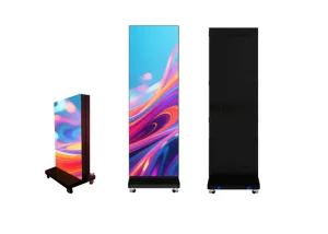
Recommended Pitch: P1.87 to P2.5 (Poster & Holographic Series)
Key Requirements: Ultra-thin profile, modular front-access maintenance, plug-and-play cloud content management via Wi-Fi/4G, and interactive capacitive touch functionality.
Navigating international trade barriers requires strict adherence to international electrical safety and electromagnetic standards. As a certified OEM/ODM exporter, all JINGRUNS high-density display series comply with major global regulatory benchmarks:
Ensures electromagnetic compatibility, permitting installation in residential and commercial zones without radio interference.
Meets rigorous North American electrical safety and fire retardancy specifications for building code integration.
100% hazardous substance restriction compliance, utilizing lead-free solder alloys and eco-friendly polymer coatings.
Complete dust protection and water jet resistance, verified by atmospheric stress testing chambers.
When evaluating wholesale quotes from China manufacturers, enterprise buyers must calculate lifetime costs beyond the initial hardware purchase ($CapEx$):
By choosing JINGRUNS Common Cathode panels and COB encapsulation, enterprise clients save up to 35% in operational electricity costs and reduce module replacement frequency by over 50% across a 5-year lifecycle.
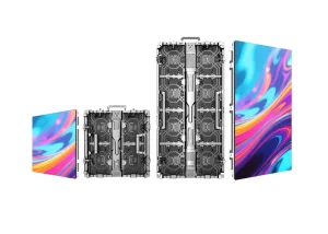
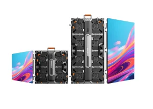
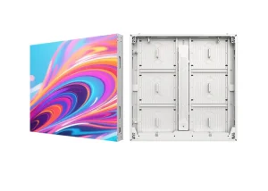
Explore our specialized outdoor, fine pitch, poster, and holographic transparent LED solutions designed for maximum commercial return.
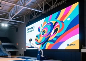
Direct engineering answers to technical and commercial questions raised by global AV integrators and procurement directors.
Contact our senior optoelectronic engineering team today for technical consultations, customized pitch calculations, project bill of materials (BOM) estimates, and factory-direct wholesale quotations.